
SEM Nanoprobing and Electrical Failure Analysis


SEM Nanoprobing and Electrical Failure Analysis
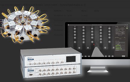
Device characterization, and failure localization and understanding in one streamlined workflow
Developed by Imina Technologies and point electronic, this system includes an advanced Electrical Failure Analysis (EFA) system fully integrated into a nanoprobing solution, suitable for any Scanning Electron Microscope (SEM), Focused Ion Beam (FIB) and Dual Beam microscopes.
It enables to visualize and analyze electrical properties and failures across the broad range of devices, components, and materials, including the most advanced technology nodes that demand low-kV and short working distance or immersion mode operation.
Key features
-
Nanoprobing: reliable electrical contact with highly stable nanoprobers offering sub-nm precision over cm range
-
Device characterization: Measurement of IV, leakage, conductance, resistance, and capacitance with advanced software and automated workflows
-
Fault localization with Electron Beam Induced Current (EBIC), Electron Beam Absorbed Current (EBAC), Resistive Contrast Imaging (RCI) and Electron Beam Induced Resistance Change (EBIRCh) technique
-
Advanced technologies: Maximize performance, speed up your process, and enable correlative analysis
To learn more visit Point Electronic >